 |
| ||||||||||||||||||||||||||||||||||||||||||||||||||||||||||||||||||||||||||||||||||||||||||||||||||||||||||||||||||||||||||||||||||||||||||||||||||||||||||||||||||||||||||||||||||||||||||||||||||||||||||||||||||||||||||||||||||||||||||||||||||||||||||||||||||||||||||||||||||||||||||||||||||||||||||||||||||||||||||||||||||||||||||||||||||||||||||||||||||||||||||||||||||||||||||||||||||||||||||||||||||||||||||||||||||||||||||||||||||||||||||||||||||||||||||||||||||||||||||||||||||||||||||||||||||||||||
|
| ||||||||||||||||||||||||||||||||||||||||||||||||||||||||||||||||||||||||||||||||||||||||||||||||||||||
Lehr- und Lernmittel,
Informationen, Beratung
Educational Aids
Literature, Consulting
Moyens didactiques,
Informations, Service-conseil
Material did�ctico,
Informaciones, Asesor�a
GTZ
Deutsche Gesellschaft f�r Technische Zusammenarbeit (GTZ) GmbH
Andreas Lange
Digital Teaching Aid
91-34-0308/2
Figure
Andreas Lange, DED,
1994
Philippines
|
| ||||||||||||||||||||||||||||||||||||||||||||||||||||||||||||||||||||||||||||||||||||||||||||||||||||||
Preface
Nearly two years ago the German Development Service (DED) offered me the possibility to assist a technical college in the Philippines.
I had finished my studies in electronic engineering in Germany and had gained several years of working experience in the development of medical electronic equipment and the organization of telecommunication units.
Since I have been assigned with the Don Bosco Technical College, I have been teaching in electronics, computer science, and have been working in the training for instructors.
One of the mayor problems I encountered was the lack of preparation time for the lessons. Many teachers are under steady time pressure because they have to serve two or more jobs in order to earn the adequate income. That gave me the idea to develop a ready-made lesson preparation for teachers.
Based on my experience and also due to the visit of many other schools I edited and compiled this Teaching Aid. I tried to integrate practice and theory which is the best way to provide a solid foundation. I hope this will support the teachers as well as it can improve the quality of classes.
Canlubang, Philippines
February 1994Andreas Lange
|
| ||||||||||||||||||||||||||||||||||||||||||||||||||||||||||||||||||||||||||||||||||||||||||||||||||||||
Introduction
This Teaching Aid is addressed to teachers and schools which offer any kind of electronic courses (i.e. computer maintenance, machine control, radio and tv repair, etc). It provides the basic knowledge for technicians as well as it can be used to run basic courses at technical colleges.
Digital Teaching Aid is a teaching module made for teachers. It is a ready - made lesson preparation and not a textbook. Therefore, you (the teacher) should already have some background knowledge on digital electronics. This module gives you all the material you need to run a course in basic digital electronics.
The module is divided into lessons, each lesson is headed by a lesson plan followed by boardscripts, worksheets, and handouts. It also contains three evaluations which you can use as tests/exams or as advanced exercises. The lesson plans are not only containing the contents of the lesson, but also gives you the objectives and suggested methods and ways to carry out the lesson. The following informs you about the purpose of every lesson plan column:
|
Time |
- The 'Time' column is still blank, it is up to you to decide how much time you would like to spend on each topic. The average time per lesson is approximately 90 minutes and 45 minutes for the review exercise (Worksheet). |
|
Method |
- The 'Method' column suggests a sample of teaching methods. Lesson plan 1 and 2 are already filled up to give you an example on how to use this column. I recommend the use of abbreviations, the meaning of every abbreviation is given at the bottom of every method column. |
|
Topic |
- The 'Topic' column gives you a brief description of the contents of every lesson. Feel free to add or drop some topics. Every topic is handled in the following boardscript pages. |
|
Way |
- The 'Way' column suggests a sample of teaching tools. Lesson plan 1 and 2 are already filled up. The explanation for the abbreviation used is given at the bottom of every way column. The boardscript pages of every lesson contain examples (EX) and hands on (HO) exercises. The HO's should be carried out by the students during the lesson. |
|
Remark |
- The 'Remark' column provides you with space for additional information. (i.e.: Where can I find the transparency/picture which I decided to use, or: What is the filename of the demo program which I already prepared) |
|
| ||||||||||||||||||||||||||||||||||||||||||||||||||||||
Digital Teaching Aid (DED Philippinen, 86 p.)
Fundamental Logic Operations - Lesson 1
Lesson Plan
Titel: Fundamental Logic Operations
Objectives:
- Understand the principle of NOT, AND, OR operations
- Able to convert binary and decimal numbers
|
Time |
Method |
Topic |
Way |
Remark | |
| |
S,D |
* Introduction |
Ex | | |
| | |
|
- Analog and digital signals | | |
| |
S,Q/A |
* Review |
B | | |
| | |
|
-Transistor in hard saturation | | |
| | |
|
- Inverter function |
| |
| |
S,D |
*TTL circuits |
B | | |
| | |
|
-History | |
|
| | | |
- Standards |
| |
| |
S |
* Logic operations |
B | | |
| |
S,E | |
-NOT |
HO |
Handout No. 1 (Family of TTL devices) |
| |
S,E | |
-AND |
EX | |
| |
S,E | |
-OR |
EX | |
| |
E |
* Binary number system |
WS |
Worksheet No. 1 | |
| |
S: Speech | |
B: Boardscript | | |
Introduction
Fundamental Logic Operations
Digital Electronics
The world of electronics is divided into two areas: analog and digital. Analog circuits consist mainly of amplifiers for voltage or current variations that are smooth and continuous. Digital circuits provide electronic switching of voltage pulses. A pulse has abrupt changes between two extreme amplitude levels (i.e.: 5 volt = high level and 0 volt = low level).
Since the digital signal has only two significant levels, either high or low, it is useful to represent the pulses in a binary number system with the digits 1 and 0. (see also Worksheet 1, Binary number system)
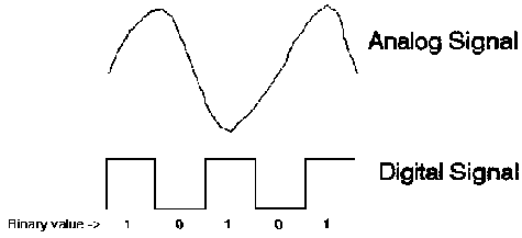
Fig. 1-1: Analog versus digital
signals
Transistor in digital electronic
A transistor can be used in analog and digital electronic. In digital electronic the transistor operates usually in hard saturation. (see also Amplifier Teaching Aid, Transistor as switch)
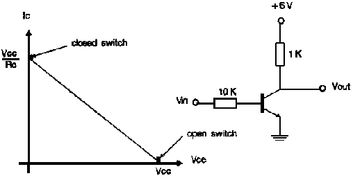
Fig. 1-2: Load line and circuit
for a transistor switch
Hard Saturation
To get hard saturation, a designer makes IC approximately 10 times the value of IB.
When the max. Vin equals to the supply voltage you can get hard saturation by using a ratio of:
10:1 for RB/RC
Inverter Function
A transistor switch (circuit as above) can be used to build the first device in digital electronic, the inverter:
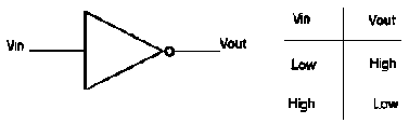
Fig. 1-3: Inverter symbol and
truth table
Because in digital electronics mainly ready made devices are used (Integrated circuits IC), we don't care any more how the single device is built up. From now on we will use only these ready made devices.
TTL circuits
1964 TEXAS Instruments introduced a family of digital devices which became standard elements in digital electronic: The TTL (Transistor Transistor Logic) circuits. The High (1) and Low (1) state is represented by voltage levels.
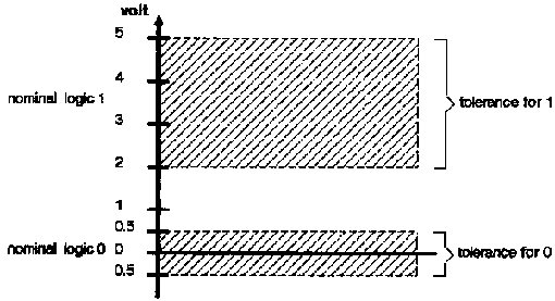
Fig. 1-4: Voltage levels for high
and low state in TTL
IC's
Logic operations
All decisions and operations can be realized by means of the three basic operations:
NOT, AND, OR
NOT (Inverter)
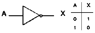
Fig. 1-5: NOT (Inverter) symbol
and truth table
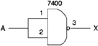
Circuit example: 7404 TTL device (see Handout No. 1)
HO: A 1KHz square wave drives pin 1 of a 7404. What does the voltage waveform at pin 2 look like?
Solution:
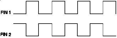
Fig. 1-6: Timing diagram, Inverter
input (pin 1) and output (pin 2)
AND gates
AND operation: The output supplies an high (1) signal if to all inputs high (1) signals are applied.
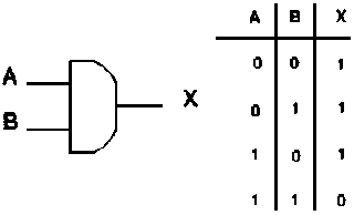
Fig. 1-6: AND symbol and truth
table
AND application example: An elevator motor may only start to work if the doors are shut AND an operation occured.
Circuit example: TTL device 7408, two input AND gate
Ex: Develop the truth table for the following logic circuit.
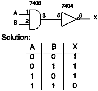
Fig. 1-8: Logic circuit with truth
table
OR gates
OR operation: An OR operation supplies a high signal at the output if to one or more inputs high signals are applied.
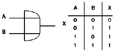
Fig. 1-9: OR gate, symbol and
truth table
OR application example: A pump has to be switched on when the water level has fallen to a certain level OR too much water is taken out of the container.
Circuit example: TTL device 7432, two input OR gate
Ex: Develop the truth table for the following logic circuit.
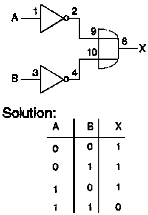
Fig. 1-10: Logic circuit with truth
table
Handout No. 1
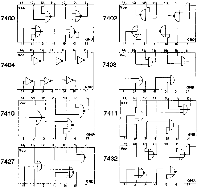
The 7400 Family of TTL Devices (Sample List)
|
Device number |
Description |
|
7400 |
Quad 2 input NAND gates |
|
7402 |
Quad 2 input NOR gates |
|
7404 |
Hex inverter |
|
7408 |
Quad 2 input AND gates |
|
7410 |
Triple 3 input NAND gates |
|
7411 |
Triple 3 input AND gates |
|
7427 |
Triple 3 input NOR gates |
|
7432 |
Quad 2 input OR gates |
Figure
Worksheet No. 1
Binary number system
All number systems have a base, which specifies how many digits can be used in each place count. For binary numbers the base is 2, with 0 and 1 as the only two digits. In the decimal system, the base is 10.
Decimal digits: 0, 1, 2, 3, 4, 5, 6, 7, 8, 9
Binary digits: 0, 1
Decimal to Binary Conversion
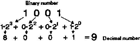
EX: Convert a 4 bit binary number
(100 1) into decimal.
Each digit position has specified weight, for binary numbers the position represents a power of two.
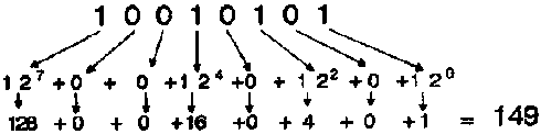
EX: Convert a 8 bit number (10010101)
into decimal
HO: Convert the following binary numbers into decimal:
101, 1100, 1110, 1000, 0110, 11001010, 01101111, 10001100
Binary to decimal conversion
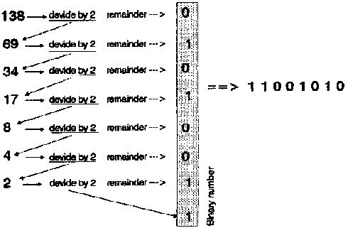
EX: Convert the decimal number 138
into a binary number
HO: Convert the following decimal numbers into binary numbers:
12, 8, 127, 247, 139, 255
|
| ||||||||||||||||||||||||||||||||||||||||||||||||||||||
Digital Teaching Aid (DED Philippinen, 86 p.)
Introduction Boolean Algebra - Lesson 2
Lesson Plan
Introduction
Titel: Introduction Boolean Algebra
Objectives:
- Able to express the basic operations in Boolean algebra
- Know how to describe a logic circuit in a Boolean equation
- Understand the basic Boolean theorems.
|
Time |
Method |
Topic |
Way |
Remark | ||
| |
Q/A |
* Review Lesson 1 |
B | | ||
| |
S |
* Introduction - George Boole |
B | | ||
| |
S |
* Boolean algebra |
B,Ex | |
||
| | |
S,E | |
- NOT operation |
| |
| | |
| |
- OR operation |
| |
| | |
| |
- AND operation |
| |
| | |
S,E | |
- Boolean equations of logic circuits |
B,Ex | |
| | | | |
- NOR gates Truth table |
B | |
| | |
S,D | |
- De Morgan's 1. theorem |
B | |
| | |
| |
- NAND gates Truth table |
B | |
| | |
E | |
- De Morgan's 2. theorem |
B,HO | |
| |
E |
* Review Exercise |
WS |
Worksheet No. 2 | ||
| |
S: Speech | |
B: Boardscript | | ||
Boolean algebra
George Boole (1854) invented a new kind of algebra that could be used to analyse and design digital and computer circuits.
NOT operation

Fig. 2-1: Inverter symbol and
Boolean notation
Ex: If A is 0 (low) ® X = NOT 0 = 1
In Boolean algebra the overbar stands for NOT operation.

OR operation
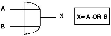
Fig. 2-2: OR symbol and Boolean
notation
Ex: If A = 0, B = 1 ® X = A or B = 0 or 1 = l
In Boolean algebra the + sign stans for the OR operation:
X = A + B
Ex: If A = 1, B = 0 ® X = A + B = 1 + 0 = 1
AND operation
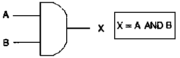
Fig. 2-3: AND symbol and Boolean
notation
In Boolean algebra the multiplication sign stands for the AND operation:
X = A · B
or simply:
X = A B
Ex: If A = 1, B = 0 ® X = A B = 1 · 0 = 0
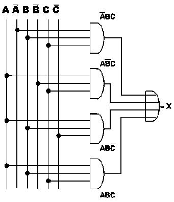
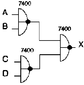
Boolean equations of logic circuits
You can use Boolean algebra as a shorthand notation for digital circuits.
Ex:
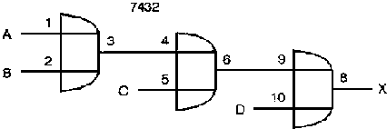
Fig. 2-4: Digital circuit
Output of the first gate:
X3 = A + B
Output of the second gate:
X6 = X3 + C = A + B + C
The final output is:
X8 = X6 + D = A + B + C + D = X
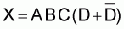
HO: Find the Boolean equation for the following circuit.

Fig. 2-5: Logic circuit
Solution:
X = (A + B) (C + D)
NOR and NAN gates
NOR gate
Based on the three fundamental logic operations it is possible to design additionel logic devices.
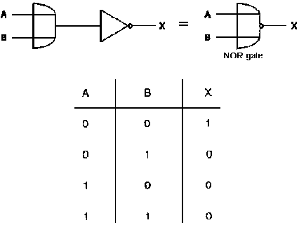
Fig. 2-6: NOR gate, symbol and
truth table
Formula: 
NAND gate
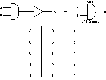
Fig. 2-7: NAND grate, symbol and
truth table
Formula: 
De Morgan's theorems
Augustus De Morgan was the first who found the link between logic and mathematics.

Fig. 2-8: Logic circuits with the
same output
Although the circuits are different but the output, as we can see in the truth table, is equal. Therefore we can write:

De Morgan's First Theorem
Also if we compare the two circuits on the next page we can easily see that the output is the same, although the circuits are different.
(see Fig. 2-9)
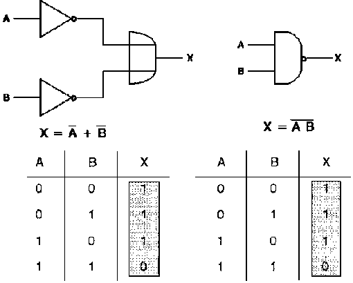
Fig. 2-9: Logic circuits with the
same output
So we can write:

De Morgan's Second Theorem
HO: How can you connect a NAND gate to get an inverter
Solution:
Figure
HO: How can you connect NAND gates to get an OR gate?
Solution:

Figure
Worksheet No. 2

No. 1 What is the
Boolean equation? What is the truth table?

No. 2 What is the
Boolean equation? What is the truth table?
No. 3 What is the
Boolean equation? What is the truth table?
No. 4 Construct the
truth table.
No. 5 Draw the logic circuit whose Boolean equation is

Use the 7404 and the 7432 with pin numbers
No. 6 Draw the logic circuit whose Boolean equation is
Use the 7404, 7432 and the 7411 with pin numbers.
|
| ||||||||||||||||||||||||||||||||||||||||||||||||||||||||||||
Digital Teaching Aid (DED Philippinen, 86 p.)
Circuit Analysis and Design - Lesson 3
Lesson Plan
Titel: Circuit Analysis and Design
Objectives:
- Know how to apply the basic Boolean laws
- Able to create digital circuits with the help of the sum of products method
|
Time |
Method |
Topic |
Way |
Remark | |
| |
|
* Review Lesson 2 |
| | |
| | |
* Introduction |
| | |
| | |
* Boolean laws and theorems |
HO |
Handout No. 2 (Boolean Algebra Theorems) | |
| | |
|
- Basic laws |
| |
| | |
|
- Boolean relation about OR operations | |
|
|
| | |
- Boolean relations about AND operations | |
|
|
| |
* Sum of products method | | | |
| | |
|
- Fundamental products | | |
| | |
|
- Sum of products equations | | |
| | |
* Review Exercise |
WS |
Worksheet No. 3 | |
| |
S: Speech | |
B: Boardscript | | |
Introduction
Circuit Analysis and Design
Boolean laws and theorems
Basic laws
(see also Handout No. 2)
Commutative law:
A + B = B + AA B = B A

Fig. 3-1: Commutative law
Associative law:
A + (B + C) = (A + B) + CA (B + C) = (A B) C

Fig. 3-2: Associative law
Distributive law:
A (B + C) = AB + AC

Fig. 3-3: Distributive law
Boolean relations about OR operations
A + 0 = A
Proof:
when A is 0
0 + 0 = 0
when A is 1
1 + 0 = 1
A + A = A
Proof:
when A is 0
0 + 0 = 0
when A is 1
1 + 1 = 1
A + 1 = 1
Proof:
when A is 0
0 + 1 = 1
when A is 1
1 + 1 = 1
A + A = 1
If one input is high, the output is high no matter what the other input is.
Boolean relations about AND operations
A · 1 = A
A · A = A
A · 0 = 0
HO: Check the equations above in the same way as we did it before.
A · A = 0
If one input is low, the output is low no matter what the other input is.
Double inversion

De Morgan's theorems
see also Lesson 1

Duality theorem
1. Change each OR sign to an AND sign
2. Change ech AND sign to an OR sign
3. Complement any 0 or 1 appearing in the expression
|
Ex: | |
A + 0 = A |
| |
® |
A 1 = A |
|
Ex: | |
A (B + C) = AB + AC |
| |
® |
A + B C = (A + B) (A + C) |
TIP: Proof it with a truth table
Ex: Simplify the following Boolean equation

Solution: (see also Handout No. 2)
|
|
Handout 2 |
No. 3a |
|
X = A (1) | |
No. 8a |
|
X = A | |
No. 7b |

HO: Simplify the following Boolean equation

Solution:


X = B + B
X = B

Sum of product method
Fig. 3-4: Example truth table with fundamental products
|
A |
B |
X |
Fundamental Products |
|
0 |
0 |
0 |
|
|
0 |
0 |
1 |
|
|
0 |
1 |
0 |
|
|
0 |
1 |
1 |
|
|
1 |
0 |
0 |
|
|
1 |
0 |
1 |
|
|
1 |
1 |
0 |
|
|
1 |
1 |
1 |
|


Design example
Sum of products equation
Given is the following truth table:
Fig. 3-5: Example truth table
|
A |
B |
C |
X | |
|
|
0 |
0 |
0 |
0 | | |
|
0 |
0 |
1 |
0 | | |
|
0 |
1 |
0 |
0 | | |
|
0 |
1 |
1 |
1 |
® |
|
|
1 |
0 |
0 |
0 | | |
|
1 |
0 |
1 |
1 |
® |
|
|
1 |
1 |
0 |
1 |
® |
|
|
1 |
1 |
1 |
1 |
® |
|


We have to locate each output 1 in the truth table and write down the fundamental product.
The next step is to OR the fundamental products:

Now we can derive the corresponding logic circuit:

Fig. 3-6: Logic circuit
HO: What is the sum of product circuit for the given truth table?
Fig. 3-7: Truth table
|
A |
B |
C |
X |
|
0 |
0 |
0 |
1 |
|
0 |
0 |
1 |
0 |
|
0 |
1 |
0 |
1 |
|
0 |
1 |
1 |
0 |
|
1 |
0 |
0 |
1 |
|
1 |
0 |
1 |
0 |
|
1 |
1 |
0 |
1 |
|
1 |
1 |
1 |
0 |
Handout No. 2
Boolean Algebra Theorems
|
No |
Theorem |
Name |
|
1a |
A + B = B + A |
Commutative law |
|
2a |
(A + B) + C = A + (B + C) |
Associative law |
|
3a |
A (B + C) = AB + AC |
Distributive law |
|
4a |
A + A = A |
Identity law |
|
5a |
|
Negation |
|
6a |
A + AB = A |
Redundancy |
|
7a |
0 + A = A | |
|
8A |
| |
|
9a |
| |
|
10a |
|
De Morgan's laws |


Worksheet No. 3
No. 1 Simplify the Boolean equation and discribe the logic circuit:

No. 2 Simplify the following Boolean expressions:

No. 3 A digital system has a 4-bit input from 0000 to 1111. Design a logic circuit that produces a high output whenever the equivalent decimal input is greater than 13.
No. 4 In a heating plant the burner X has to be switched on, when the circulating pump A is actuated and the temperature probe B for the warm water supply or the room temperature probe C respond.
a) Develop the truth table
b) Write down the sum of products equation
c) Draw the logic circuit
d) Use Boolean algebra to simplify the equation
e) Draw the corresponding logic circuit.
|
| ||||||||||||||||||||||||||||||||||||||||||||||||||||||||||||||||||||||||||||||||||||||||||||||||||||||
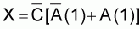
First Evaluation
No. 1 Construct the truth Table
What is the Boolean equation?

Figure
No. 2 Draw the logic circuit whose Boolean equation is

Use the 7404, 7408 and the 7411 with pin numbers
No. 3 Simplify the following Boolean expressions

No. 4 A digital system has a 4 bit input from 0000 to 1111.
Design a logic circuit that produces a high output whenever the equivalent hex input is greater than C.
Truth table
Sum of products equation
Logic circuit
No. 5
|
A |
B |
C |
D |
Y |
|
0 |
0 |
0 |
0 |
0 |
|
0 |
0 |
0 |
1 |
1 |
|
0 |
0 |
1 |
0 |
0 |
|
0 |
0 |
1 |
1 |
0 |
|
0 |
1 |
0 |
0 |
0 |
|
0 |
1 |
0 |
1 |
1 |
|
0 |
1 |
1 |
0 |
1 |
|
0 |
1 |
1 |
1 |
1 |
|
1 |
0 |
0 |
0 |
0 |
|
1 |
0 |
0 |
1 |
1 |
|
1 |
0 |
1 |
0 |
1 |
|
1 |
0 |
1 |
1 |
1 |
|
1 |
1 |
0 |
0 |
0 |
|
1 |
1 |
0 |
1 |
1 |
|
1 |
1 |
1 |
0 |
1 |
|
1 |
1 |
1 |
1 |
0 |
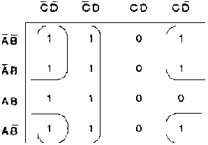
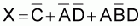
a) Draw the Karnaugh map
b) Encircle all octets, quads, and
pairs you can find.
c) What is the simplified Boolean equation?
d) Draw
the logic circuit using NAND
gates.
|
| ||||||||||||||||||||||||||||||||||||||||||||||||||||||||||||
Digital Teaching Aid (DED Philippinen, 86 p.)
Karnaugh Mapping - Lesson 4
Lesson Plan
Titel: Karnaugh Mapping
Objectives:
- Able to derive Karnaugh maps from a given truth table
- Know how to simplify Karnaugh maps
|
Time |
Method |
Topic |
Way |
Remark | |
| |
|
* Review Lesson 3 |
| | |
| | |
* Introduction |
| | |
| | |
|
- Karnaugh map |
| |
| | |
* Karnaugh mapping |
| | |
| | |
|
- Truth table to Karnaugh map | | |
| | |
|
- Two variable map |
| |
| | |
|
- Three variable map |
| |
| | |
|
- Four variable map |
| |
| | |
|
- Pairs, Quads, and Octets | | |
| | |
|
- Overlapping groups |
| |
| | |
|
- Rolling the map |
| |
| | |
* Review exercise |
WS |
Worksheet No. 4 | |
| |
S: Speech | |
B: Boardscript | | |
Introduction
Karnaugh Mapping
Simplify a Boolean equation
|
Ex: |
| |
| |
|
|
|
|
|
Again factor to get |
| |
|
Simplify |
| |
|
Simplify |
| |
| |
 is common in each
term
is common in each
term 


Karnaugh map
As you see, Boolean algebra can be used to create simpler circuits. But if you not quite familiar with Boolean theorems it is difficult to find the best simplification. Therefore Karnaugh mapping is the better alternative for simplification.
Truth table to Karnaugh map
The starting point for digital circuit design is usually the truth table which gives us the following information:
Under which input condition occurs a certain output condition.
Two variable map
Ex:

Fig. 4-1: Two variable Karnaugh
map
The truth table outputs are translated into the Karnaugh map. Each position in the map represents a certain fundamental product.
Three variable map
Ex:
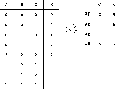
Fig. 4-2: Three variable Karnaugh
map
Four variable map
Many digital systems process 4 bit numbers. For this reason, logic circuits are often designed to handle 4 input variables.
Ex:
(see Fig. 4-3)
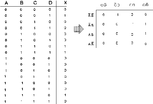
Fig. 4-3: Four variable Karnaugh
map
Pairs, Quads, and Octets
Pairs
Fig. 4-4: Four variable
simplification
As you see in Fig. 4-4, only one variable goes from uncomplement to complement. Whenever this happens, you can eliminate the variable that changes form.
|
Proof: |
|
| |
|
| |
X = A B C |

Ex:
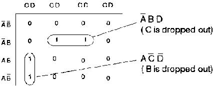
Fig. 4-5: Pairs
Whenever you see a pair first encircle it and then simplify to get the simplified Boolean expression:

Quad
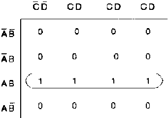
Fig. 4-6: Quad
Quad: A group of 4 one's that are horizontally or vertically adjacent. End to end or in form of a square.
A quad eliminates two variables and their complements.
|
Proof: |
|
(two pairs) |
| |
X = A B (C + C) |
|
|
|
X = A B | |
Encircle the quad and step through the different one's in the quad and determine which two variables go from complement to uncomplement (or vs), these are the variables that drop out.
Ex:
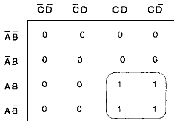
Fig. 4-7: Quad
The variables B and D can be eliminated. So we get the following equation:
X = A C
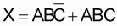
Octet
Fig. 4-8: Octet
An octet eliminates three variables and their complements.
|
Proof: |
|
(two quads) |
| |
X = A (C + C) |
|
|
|
X = A | |
Karnaugh Simplifications
Process:
1. Draw the Karnaugh map
2. Look for octets and encircle them.
3. Look for quads and encircle them.
4. Look for pairs and encircle them.
5. Simplify and write down the equation.
Ex:
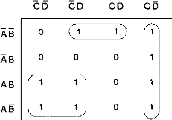
Fig. 4-9: Karnaugh map

Overlapping and Rolling
Overlapping groups
Ex:
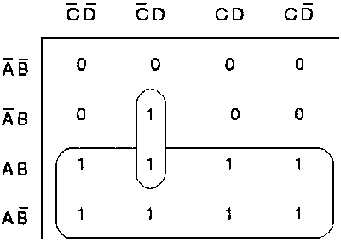
Fig. 4-10: Karnaugh map
Groups can overlap to get a simpler equation:
Rolling the map
Ex:
Fig. 4-11: Karnaugh map
Instead of encircling two pairs:
We can roll the map and encircle a quad:

HO: Simplify the following
map.
Solution:
HO: Simplify the following
map.
Solution:
Worksheet No. 4
No. 1 Simplify the following Karnaugh maps and write down the Boolean equation for every map.
| |
|
|
|
|
0 |
0 |
|
|
1 |
0 |
|
|
1 |
1 |
|
|
0 |
0 |


| |
|
|
|
|
1 |
1 |
|
|
0 |
0 |
|
|
1 |
0 |
|
|
1 |
1 |


| |
|
|
|
|
1 |
0 |
|
|
0 |
0 |
|
|
0 |
0 |
|
|
1 |
0 |


| |
|
|
|
|
|
|
0 |
1 |
0 |
0 |
|
|
1 |
0 |
1 |
1 |
|
|
1 |
0 |
0 |
1 |
|
|
0 |
1 |
1 |
0 |


| |
|
|
|
|
|
|
1 |
1 |
0 |
1 |
|
|
0 |
0 |
1 |
1 |
|
|
0 |
0 |
0 |
1 |
|
|
1 |
1 |
0 |
1 |


No. 2 Translate each output (v, w, x, y, z) into a Karnaugh map, do the simplification and write down the Boolean equation.
|
A |
B |
C |
D |
v |
w |
x |
y |
z |
|
0 |
0 |
0 |
0 |
1 |
1 |
0 |
1 |
0 |
|
0 |
0 |
0 |
1 |
0 |
1 |
0 |
1 |
1 |
|
0 |
0 |
1 |
0 |
0 |
1 |
0 |
0 |
0 |
|
0 |
0 |
1 |
1 |
0 |
0 |
0 |
0 |
1 |
|
0 |
1 |
0 |
0 |
0 |
0 |
1 |
0 |
1 |
|
0 |
1 |
0 |
1 |
1 |
0 |
1 |
1 |
0 |
|
0 |
1 |
1 |
0 |
1 |
1 |
1 |
1 |
0 |
|
0 |
1 |
1 |
1 |
1 |
0 |
1 |
1 |
0 |
|
1 |
0 |
0 |
0 |
0 |
1 |
0 |
0 |
1 |
|
1 |
0 |
0 |
1 |
1 |
1 |
1 |
1 |
0 |
|
1 |
0 |
1 |
0 |
0 |
1 |
0 |
1 |
0 |
|
1 |
0 |
1 |
1 |
1 |
1 |
1 |
1 |
1 |
|
1 |
1 |
0 |
0 |
0 |
0 |
0 |
0 |
1 |
|
1 |
1 |
0 |
1 |
1 |
0 |
0 |
0 |
1 |
|
1 |
1 |
1 |
0 |
0 |
0 |
0 |
1 |
1 |
|
1 |
1 |
1 |
1 |
0 |
1 |
0 |
0 |
0 |
|
| ||||||||||||||||||||||||||||||||||||||||||||||||
Digital Teaching Aid (DED Philippinen, 86 p.)
Karnaugh Mapping II - Lesson 5
Lesson Plan
Titel: Karnaugh Mapping II
Objectives:
- Understand the product of sums method
- Able to use “Don't care conditions” for more effective simplifications
|
Time |
Method |
Topic |
Way |
Remark | |
| |
|
* Review Lesson 4 |
| | |
|
|
|
* Introduction |
| | |
|
|
|
* Product of sums method | | | |
|
|
| |
- Fundamental sums |
| |
|
|
| |
- Product off sums simplifications | | |
|
|
|
* Don't care conditions | | | |
|
|
| |
-Truth table |
| |
|
|
| |
- Karnaugh map |
| |
|
|
|
* Review exercise |
|
Worksheet No. 5 | |
|
|
S: Speech | |
B: Boardscript | | |
Introduction
Karnaugh Mapping II
Product of sums method
Instead of using the sum of products method we can also take the product of sums method which is based on the fundamental sums:
Fig. 5-1: Truth table with fundamental sums
|
A |
B |
C |
X | |
Fundamental sums |
|
0 |
0 |
0 |
0 |
® |
|
|
0 |
0 |
1 |
1 | | |
|
0 |
1 |
0 |
1 | | |
|
0 |
1 |
1 |
0 |
® |
|
|
1 |
0 |
0 |
1 | | |
|
1 |
0 |
1 |
1 | | |
|
1 |
1 |
0 |
0 |
® |
|
|
1 |
1 |
1 |
1 | | |


Product of sums simplification
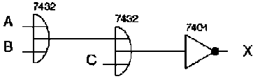
A equation gained through the sum of product method can be realized into a NAND-NAND logic circuit.

Fig. 5-2: NAND-NAND logic
circuit
If we simplify the Karnaugh map in Fig. 5-2 we get the following equation:

Based on this equation we can draw the logic circuit like in Fig. 5-2. This solution is made with the help of the sum of product method. If we want to try the product of sums method we have to go through the following steps:
1. Complement the Karnaugh map and draw the complementary NAND-NAND circuit:

Fig. 5-3: Complementary NAND-NAND
circuit
The simplified equation is:

2. Convert the complementary NAND-NAND circuit to a NOR-NOR circuit:

Fig. 5-4: NOR-NOR circuit
we have changed all NAND to NOR and complemented all signals.
3. Now we got a product of sums solution for X. The last step is to compare both circuits (NAND-NAND, NOR-NOR) to find out which circuit is the simpler one, meaning the cheaper one. Because we need less gates. In our case the sum of product solution (NOR-NOR circuit) is the better solution.
Summary of process
1. Convert the truth table into a Karnaugh map
- Write the sum of products equation
- Draw the NAND-NAND circuit
2. Complement the Karnaugh map
- Draw the complementary NAND-NAND circuit

3. Convert the complementary NAND-NAND circuit to a NOR-NOR circuit.
- Change all NAND to NOR
- Complement all signals
4. Compare NAND-NAND circuit with NOR-NOR circuit.
Don't care conditions
In some digital systems, certain input conditions never occur during normal operations; therefore, the corresponding output never appears.
Þ It is indicated in the truth table by an X.
Fig. 5-5: Don't care conditions
|
A |
B |
C |
D |
Z | |
|
0 |
0 |
0 |
0 |
0 | |
|
0 |
0 |
0 |
1 |
0 | |
|
0 |
0 |
1 |
0 |
0 | |
|
0 |
0 |
1 |
1 |
0 | |
|
0 |
1 |
0 |
0 |
0 | |
|
0 |
1 |
0 |
1 |
0 | |
|
0 |
1 |
1 |
0 |
0 | |
|
0 |
1 |
1 |
1 |
0 | |
|
1 |
0 |
0 |
0 |
0 | |
|
1 |
0 |
0 |
1 |
1 | |
|
1 |
0 |
1 |
0 |
X | |
|
1 |
0 |
1 |
1 |
X | |
|
1 |
1 |
0 |
0 |
X |
Don't care conditions |
|
1 |
1 |
0 |
1 |
X | |
|
1 |
1 |
1 |
0 |
X | |
|
1 |
1 |
1 |
1 |
X | |
Don't care conditions are like wild cards, you can let them stand for what ever you like:

Fig. 5-6: Karnaugh map and
simplified equation
HO: Simplify the following Boolean function:

That has the don't care conditions:

Solution:
First we have to translate the function into a truth table:
|
W |
X |
Y |
Z |
F |
|
0 |
0 |
0 |
0 |
X |
|
0 |
0 |
0 |
1 |
1 |
|
0 |
0 |
1 |
0 |
X |
|
0 |
0 |
1 |
1 |
1 |
|
0 |
1 |
0 |
0 |
0 |
|
0 |
1 |
0 |
1 |
X |
|
0 |
1 |
1 |
0 |
0 |
|
0 |
1 |
1 |
1 |
1 |
|
1 |
0 |
0 |
0 |
0 |
|
1 |
0 |
0 |
1 |
0 |
|
1 |
0 |
1 |
0 |
0 |
|
1 |
0 |
1 |
1 |
1 |
|
1 |
1 |
0 |
0 |
0 |
|
1 |
1 |
0 |
1 |
0 |
|
1 |
1 |
1 |
0 |
0 |
|
1 |
1 |
1 |
1 |
1 |
Now we have to convert it into a Karnaugh map and simplify it:

Figure
Worksheet No. 5
No. 1
|
A |
B |
C |
D |
Y |
|
0 |
0 |
0 |
0 |
0 |
|
0 |
0 |
0 |
1 |
1 |
|
0 |
0 |
1 |
0 |
0 |
|
0 |
0 |
1 |
1 |
0 |
|
0 |
1 |
0 |
0 |
0 |
|
0 |
1 |
0 |
1 |
1 |
|
0 |
1 |
1 |
0 |
0 |
|
0 |
1 |
1 |
1 |
0 |
|
1 |
0 |
0 |
0 |
0 |
|
1 |
0 |
0 |
1 |
0 |
|
1 |
0 |
1 |
0 |
1 |
|
1 |
0 |
1 |
1 |
1 |
|
1 |
1 |
0 |
0 |
1 |
|
1 |
1 |
0 |
1 |
1 |
|
1 |
1 |
1 |
0 |
1 |
|
1 |
1 |
1 |
1 |
1 |
a) Draw the Karnaugh map.
b) Encircle all octets, quads and pairs you can find.
c) What is the simplified Boolean equation for the Karnaugh map?
d) Draw the logic circuit.
e) Suppose the last six entries of the truth table are changed to don't cares. Using the Karnaugh map, show the simplified circuit.
f) What is the simplified NOR-NOR circuit?
|
| ||||||||||||||||||||||||||||||||||||||||||||||||||||||||||||||||||||||||
Digital Teaching Aid (DED Philippinen, 86 p.)
Coding - Lesson 6
Lesson Plan
Titel: Coding
Objectives:
- Get an idea about the purpose of codes
- Understand the principle of decoder, encoder, and code converter
- Able to design logic circuits for code conversion
|
Time |
Method 1 |
Topic |
Way |
Remark | |
| |
|
* Review Lesson 5 |
| | |
| | |
* Introduction |
| | |
| | |
* ASCII code |
| | |
| | |
|
- Coding scheme |
| |
| | |
|
- Parity bit |
| |
| | |
* BCD code | |
| |
| | |
* Excess-3 code |
| | |
| | |
* Gray code |
| | |
| | |
* Encoder | |
| |
| | | |
- Decimal to BCD encoder | | |
| | |
* Decoder | |
| |
| | | |
- BCD to decimal decoder | | |
| | |
* Code converter | | | |
| | |
|
- BCD to Exces-3 code converter | | |
| | |
* Review Exercise |
|
Worksheet No. 6 | |
| |
S: Speech |
|
B: Boardscript | | |
Introduction
Coding
Ex: Coding ® Alphanumeric information in and out of a computer.
ASCII code
ASCII Code (American Standard Code for Information Interchange)
ASCII code is a 7 bit code whose format is
X6 X5 X4 X3 X2 X1 X0
i.e. the letter A is coded as:
1 0 0 0 0 0 1
Coding scheme:
|
X6 X5 X4 | |||||||||
|
X3 |
X2 |
X1 |
X0 |
010 |
011 |
100 |
101 |
110 |
111 |
|
0 |
0 |
0 |
0 | |
0 | |
P | |
P |
|
0 |
0 |
0 |
1 | |
1 |
A |
Q |
a |
q |
|
0 |
0 |
1 |
0 | |
2 |
B |
R |
b |
r |
|
. |
. |
. |
. | |
. |
. |
. |
. |
. |
|
. |
. |
. |
. | |
. |
. |
. |
. |
. |
|
. |
. |
. |
. | |
. |
. |
. |
. |
. |
|
1 |
1 |
1 |
1 | |
|
0 | | | |
Ex; The letter B via ASCII in binary:
1 0 0 0 0 1 0
Parity bit
During sending/transmitting data, 1 bit errors may occur. To catch these errors, a parity bit is usually transmitted along with the original bits:
X7 X6 X5 X4 X3 X2 X1 X0
|
parity bit
A parity checker at the receiving end can test for even or odd parity. I.e the transmitting station will set the parity bit always in that way to put the whole number in even parity. If the parity checker at the receiving end determines odd parity it will report an error message.
Now we have 8 bits (1 byte), this is the ideal length because most digital equipment is set up to handle bytes of data.
BCD Code (Binary Coded Decimal)
Each decimal place (0...9) is represented by a binary code.
|
Ex: |
753 | | |
| |
0111 |
0101 |
0011 |
| |
7 |
5 |
3 |
The BCD code is a 4 bit code which is very common along digital systems.
Excess-3 code
Also an important 4 bit code
Ex: Convert a decimal number in excess-3 code:
|
12 ® excess-3 | ||
|
|
|
First we add 3 to every decimal digit. |
|
0100 |
0101 |
Then we convert the sum in BCD form. |
|
0100 0101 in excess-3 stands for decimal 12. | ||


Fig. 6-1: Convertion table, dec ® BCD® excess-3
|
Decimal |
BCD |
Excess - 3 |
|
0 |
0000 |
001 1 |
|
1 |
0001 |
0100 |
|
2 |
0010 |
0101 |
|
3 |
0011 |
0110 |
|
4 |
0100 |
0111 |
|
5 |
0101 |
1000 |
|
6 |
0110 |
1001 |
|
7 |
0111 |
1010 |
|
8 |
1000 |
1011 |
|
9 |
1001 |
1100 |
Gray code
Each Gray code number differs from the preceding number by a single bit.
Fig. 6-2: Convertion table, dec ® Gray ® BCD
|
Decimal |
Gray |
Binary |
|
0 |
0000 |
0000 |
|
1 |
0001 |
0001 |
|
2 |
0011 |
0010 |
|
3 |
0010 |
0011 |
|
4 |
0110 |
0100 |
|
5 |
0111 |
0101 |
|
6 |
0101 |
0110 |
|
7 |
0100 |
0111 |
|
8 |
1100 |
1000 |
|
9 |
1101 |
1001 |
Encoder
An encoder converts an active input signal into a coded output signal.
Ex: Decimal to BCD encoder
(see Fig. 6-3 on the next page) If switch 9 is pressed:
A B C D = 1 0 0 1
The circuit in Fig. 6-3 is also available as TTL device 74147.
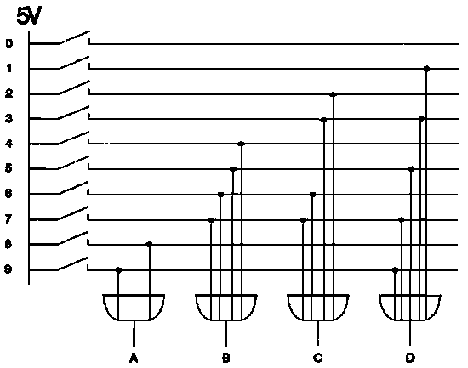
Fig. 6-3: Decimal to BCD
encoder
Decoder
A decoder converts a coded input signal into an active output signal.
Ex; Develop a decoder circuit which converts BCD code into decimal.
Fig. 6-4: Truth table, BCD ® decimal
|
a |
b |
c |
d | |
|
23 |
22 |
21 |
20 |
Dec |
|
0 |
0 |
0 |
0 |
0 |
|
0 |
0 |
0 |
1 |
1 |
|
0 |
0 |
1 |
0 |
2 |
|
0 |
0 |
1 |
1 |
3 |
|
0 |
1 |
0 |
0 |
4 |
|
0 |
1 |
0 |
1 |
5 |
|
0 |
1 |
1 |
0 |
6 |
|
0 |
1 |
1 |
1 |
7 |
|
1 |
0 |
0 |
0 |
8 |
|
1 |
0 |
0 |
1 |
9 |
To optimize the circuit we use a Karnaugh map for simplification:
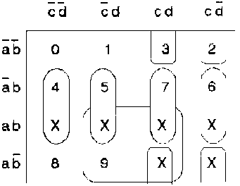
Fig. 6-5: Karnaugh map
For every number in the Karnaugh map we can write an equation:


Now we can draw the logic circuit:
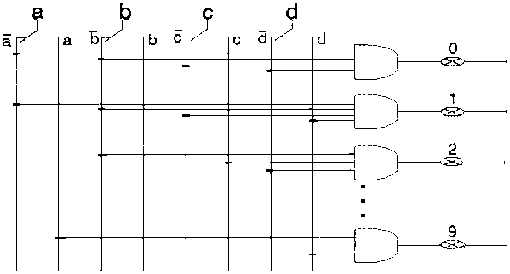
Fig. 6-6: Decoder circuit, BCD
®
decimal
Code converter
Code converter are logical networks which convert codes into another.
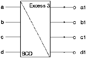
Fig. 6-7: TTL device, BCD ® excess-3 converter
Fig. 6-8: Convertion table, dec ® BCD® excess-3
|
Dec |
BCD |
Excess - 3 | ||||||
| |
a |
b |
e |
d |
a1 |
b1 |
c1 |
d1 |
|
0 |
0 |
0 |
0 |
0 |
0 |
0 |
1 |
1 |
|
1 |
0 |
0 |
0 |
1 |
0 |
1 |
0 |
0 |
|
2 |
0 |
0 |
1 |
0 |
0 |
1 |
0 |
1 |
|
3 |
0 |
0 |
1 |
1 |
0 |
1 |
1 |
0 |
|
4 |
0 |
1 |
0 |
0 |
0 |
1 |
1 |
1 |
|
5 |
0 |
1 |
0 |
1 |
1 |
0 |
0 |
0 |
|
6 |
0 |
1 |
1 |
0 |
1 |
0 |
0 |
1 |
|
7 |
0 |
1 |
1 |
1 |
1 |
0 |
1 |
0 |
|
8 |
1 |
0 |
0 |
0 |
1 |
0 |
1 |
1 |
|
9 |
1 |
0 |
0 |
1 |
1 |
1 |
0 |
0 |
Worksheet No. 6
No. 1 Develop a decoder circuit for the conversion of the Gray code into the decimal system. Use a Karnaugh map to get a simplified circuit!
|
Gray code |
decimal | |||
|
d |
c |
b |
a | |
|
0 |
0 |
0 |
0 |
0 |
|
0 |
0 |
0 |
1 |
1 |
|
0 |
0 |
1 |
1 |
2 |
|
0 |
0 |
1 |
0 |
3 |
|
0 |
1 |
1 |
0 |
4 |
|
0 |
1 |
1 |
1 |
5 |
|
0 |
1 |
0 |
1 |
6 |
|
0 |
1 |
0 |
0 |
7 |
|
1 |
1 |
0 |
0 |
8 |
|
1 |
1 |
0 |
1 |
9 |
|
X |
X |
X |
X | |
|
. |
. |
. |
. | |
|
. |
. |
. |
. | |
No. 2 Develop a code converter for the conversion of the excess 3 code into the 8421 code (BCD).
Complete the truth table!
Use Karnaugh maps to get a simplified circuit!
|
Excess 3 code |
8421 code | |||||||
|
dec |
d |
c |
b |
a |
d1 |
c1 |
b1 |
a1 |
|
0 |
0 |
0 |
1 |
1 |
0 |
0 |
0 |
0 |
|
1 |
0 |
1 |
0 |
0 |
0 |
0 |
0 |
1 |
|
2 |
0 |
1 |
0 |
1 |
0 |
0 |
1 |
0 |
|
3 |
0 |
1 |
1 |
0 |
0 |
0 |
1 |
1 |
|
4 |
0 |
1 |
1 |
1 |
0 |
1 |
0 |
0 |
|
5 |
1 |
0 |
0 |
0 |
0 |
1 |
0 |
1 |
|
6 |
1 |
0 |
0 |
1 |
0 |
1 |
1 |
0 |
|
7 |
1 |
0 |
1 |
0 |
0 |
1 |
1 |
1 |
|
8 |
1 |
0 |
1 |
1 |
1 |
0 |
0 |
0 |
|
9 |
1 |
1 |
0 |
0 |
1 |
0 |
0 |
1 |
| |
1 |
1 |
0 |
1 |
1 |
0 |
1 |
0 |
| |
1 |
1 |
1 |
0 |
1 |
0 |
1 |
1 |
| |
1 |
1 |
1 |
1 |
1 |
1 |
0 |
0 |
| |
0 |
0 |
0 |
0 |
1 |
1 |
0 |
1 |
| |
0 |
0 |
0 |
1 |
1 |
1 |
1 |
0 |
| |
0 |
0 |
1 |
0 |
1 |
1 |
1 |
1 |
The lower six rows are redundant.
|
| ||||||||||||||||||||||||||||||||||||||||||||||||||||||
Digital Teaching Aid (DED Philippinen, 86 p.)
Flip-Flops - Lesson 7
Lesson Plan
Titel: Flip-Flops
Objectives:
- Understand the Flip-Flop principle
- Know the three basic Flip-Flops (RS, D, JK)
- Able to analyze timing diagrams
|
Time |
Method |
Topic |
Way |
Remark |
| |
|
* Review Lesson 6 |
| |
| | |
* Introduction |
| |
| | |
* RS Flip-Flops |
| |
| | |
* Clocked RS-FF |
| |
| | |
* Timing diagram |
| |
| | |
* D-FF | | |
| | |
* FF switching time |
| |
| | |
* JK-FF | |
|
| | |
* JK-MS-FF | |
|
| | |
* Review exercise |
|
Worksheet No. 7 |
| |
S: Speech | |
B: Boardscript | |
Introduction
Flip-Flops
Sometimes there is a need of digital devices or circuits whose output will remain unchanged, once set, even if there is a change in input.
RS Flip-Flops
A Flip-Flop is a bistable electronic circuit that has two stable states.
Þ Output is either 0 or 5V dc
The Flip-Flop can be regarded as a memory device. It can be used to store one binary digit at the output.

Fig. 7-1: RS Flip-Flop, logic
circuit and device symbol
HO: What is the truth table for the circuit above?
Solution:
Fig. 7-2: Truth table, RS Flip-Flop
|
R |
S |
Q |
Action |
|
0 |
0 |
Last value |
No change |
|
0 |
1 |
1 |
Set |
|
1 |
0 |
0 |
Reset |
|
1 |
1 |
? |
Forbidden |
If both inputs (R, S) are high at once, the output can not be determined before; therefore, it is a forbidden state.
Ex: Create a RS Flip-Flop with NAND gates.

Fig. 7-3: RS Flip-Flop with NAND
gates
Note: The inputs (R, S) are indicated with an overbar so they are inverted.

Fig. 7-4: Logic symbol, RS
Flip-Flop with inverted inputs
Clocked RS Flip-Flop

Fig. 7-5: Clocked RS Flip-Flop
This Flip-Flop ca be enabled or disabled.
ENABLE ® low: R and S will have no effect on the output
ENABLE ® high: R and S inputs will be directly transmitted to the output

Fig. 7-6: Logic symbol, Clocked RS
Flip-Flop
Timing diagram
A timing diagram is a drawing to determine the time dependent actions of logic devices.
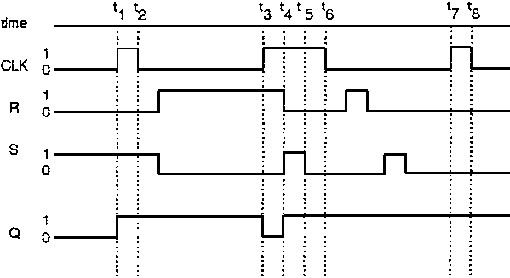
Fig. 7-7: Timing diagram of a
clocked RS Flip-Flop
Fig. 7-7 shows that the inputs (R, S) effect the output (Q) only when the clock signal (CLK) is high.
RS Flip-Flop application: Bounce free switch
D - Flip-Flop (D-FF)
The generation of two signals to drive a Flip-Flop is a disadvantage in many applications. This has led to the D-FF, a circuit that needs only a single data input.

Fig. 7-8: D Flip-Flop, logic
circuit and truth table
CLK ® low: D can change without effect on the output
CLK ® high: Q is forced to equal the value of D
Ex: Create a 4 bit data memory with D-latches (D-FF).

Fig. 7-9: Data storage with
D-FF
In Fig. 7-9, when the clock goes high, input data is loaded into the Flip-Flops and appears at the output.
Suppose the data input is:
D3 D2 D1 D0 = 1 0 1 0
When the clock goes high this 4 bit word is loaded into the D-latches, resulting in an output of:
Q3 Q2 Q1 Q0 = 1 0 1 0
Flip-Flop switching time

Fig. 7-10: Timing diagram, FF
switching time
|
tset: |
Minimum of time that the date bit must be present before the clock edge hits (because of stray capacitance) |
|
thold: |
The data bit has to be hold long enough for the internal transistors to switch. |
|
tp: |
Switching time, diodes and transistors cannot switch states immediately. (some nanoseconds) |
JK Flip-Flop (JK-FF)
Flip - Flops can be used to build counters, JK-FF are the ideal elements for that purpose.

Fig. 7-11: JK-FF, logic circuit
Ex: What is the truth table for the circuit above?
Fig. 7-12: Truth table, JK-FF
|
CLK |
J |
K |
Q |
|
X |
0 |
0 |
last state |
|
|
0 |
1 |
0 |
|
|
1 |
0 |
1 |
|
|
1 |
1 |
toggle |
|
J and K ® low: |
Both AND gates are disabled, clock pulses have no effect. Q retains its last value. |
|
J ® low, K ® high: |
The upper gate is disabled, only reset is possible (unless Q is already reset). |
|
J ® high, K ® low: |
The lower gate is disabled, only set is possible (unless Q is already high). |
|
J and K ® high: |
Set or reset is possible, the Flip-Flop will “toggle” on the next positive clock edge. Toggle means to switch to the opposite state. |
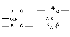
Fig. 7-13: JK-FF's, logic
symbols
Preset (PR) and Clear (CLR) are input signals to get a definite start point.
JK Master-Slave FF (JK-MS-FF)
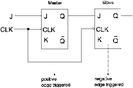
Fig. 7-14: JK-MS-FF, logic
circuit
Regardless what the master does, the slave copies it. The slave copies the master on the negative clock edge. This circuit provides a way to avoid racing.

Fig. 7-15: JK-MS-FF, logic
symbol
Available as TTL device: 74 LS 76
Worksheet No. 7
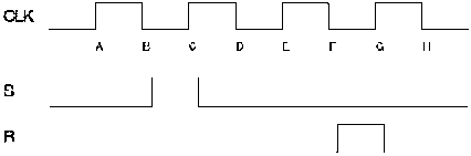
No. 1 A JK master slave FF has its inputs tied to + 5V, and a series of pulses are applied to its CLK input Describe the Q output.

Figure
No. 2 The signal drives a clocked RS - FF. If Q is low before point A in time: At what point does Q becomes a 1? What does Q reset to 0?
Figure
No. 3 Use the information in the preceding problem and draw the waveform Q.
No. 4 The signal drives a D-FF. What is the value of stored in the FF after the clock pulse is over?

Figure
No. 5 A normal JK-FF, J = K = 1. A 1 MHz is applied to the CLK input it has a propagation delay tp of 50 ns. Draw the input squarewave and the out put expected at Q. Be sure to show the propagation delay time.
|
| ||||||||||||||||||||||||||||||||||||||||||||||||||||||||||||||||||||||||||||||||||||||||||||||||||||||
Second Evaluation
No. 1 In a workshop two machines are driven by an electric motor
|
Power consumption: |
motor A = 1 KW |
| |
motor B = 2 KW |
For a new machine of which its motor C receives the power of 4 KW, the maximum main power of Pmax = 4 KW is sufficient only if the two other machines (A and B) are not switched on. Design a circuit which supplies a warning signal Q if a power higher than 4 KW is taken from the main power system by the three machines.
- Truth table
- Karnaugh map
- Logic circuit
No. 2 For a display of the figures 1-6, in the well known spot configuration of a game die, design the code conversion circuit. At the input the figures are binary coded.
T, U, V, W, X, Y, Z are output variables (LED's)
- Truth table
- Karnaugh map
- Logic circuit

Figure
No. 3 Design a JK Flip Flop with NAND and AND gates.
- Logic circuit
- Truth table
No. 4 Design a D Flip Flop. Use only NAND gates.
- Logic circuit
- Truth table
|
| ||||||||||||||||||||||||||||||||||||||||||||||||||||||
Digital Teaching Aid (DED Philippinen, 86 p.)
Counter - Lesson 8
Lesson Plan
Titel: Counter
Objectives:
- Understand the principle of asynchronous and synchronous counter
- Able to design asynchronous counter
- Know the seven segment principle
|
Time |
Method |
Topic |
Way |
Remark | |
| |
|
* Review Lesson 7 |
| | |
| | |
* Introduction |
| | |
| | |
* Asynchronous counter | | | |
| | |
|
- Timing diagram |
| |
| | |
|
- Truth table |
| |
| | |
|
- Countdown mode |
| |
| | |
* Synchronous counter | | | |
| | |
* Seven Segment Indicator and Decoder | |
| |
|
| | |
- Common anode indicator | | |
| | |
|
- Common cathode indicator | | |
| | |
|
- Seven segment decoder | | |
| | |
* Review Exercise |
|
Worksheet No. 8 | |
| |
S: Speech | |
B: Boardscript |
| |
Introduction
Counter
Counters are beside the logic operations the basic elements of all digital controls.
Since the clock pulses occur at known intervals, the counter can be used as an instrument for measuring time and therefore period or frequency.
On principle there are two counting organisations:
- Asynchronous (serial, ripple) counter
Each Flip-Flop is triggered by the previous Flip-Flop, and thus the counter has a cumulative settling time. (Delay time, tp)
- Synchronous (parallel) counter
Here, every Flip-Flop is triggered by the clock (synchronous), and thus the settling time is simply equal to the delay time of a single Flip-Flop.
Asynchronous counter

Fig. 8-1: Asynchronous counter
with JK-MS-FF in toggle mode
To understand how this counter works lets have a look at the timing diagram:

Fig. 8-2: Timing diagram,
asynchronous mod 8 counter
The frequency of waveform C is one half that at B, but is only one-eighth the clock frequency.
The FF's are negative edge triggered, hence output signals change only at the falling side of the clock pulse.
Fig. 8-3: Truth table, asynchronous mod 8 counter
|
CLK transition |
C |
B |
A |
|
0 |
0 |
0 |
0 |
|
1 |
0 |
0 |
1 |
|
2 |
0 |
1 |
0 |
|
3 |
0 |
1 |
1 |
|
4 |
1 |
0 |
0 |
|
5 |
1 |
0 |
1 |
|
6 |
1 |
1 |
0 |
|
7 |
1 |
1 |
1 |
|
0 |
0 |
0 |
0 |
A three Flip-Flop counter is often referred to as a mod 8 (modulus 8) counter since it has 8 states.
|
23 = 8 output conditions |
(The exponent equals to the number of Flip-Flops) |
The largest decimal number which is represented by a 3 Flip-Flop counter is:
|
|
23 - 1 = 7 |
|
In general: |
2n - 1 |
Count Down mode
Switching the clock inputs of each Flip-Flop to the  outputs causes the counting sequence to start at 111
down to 000.
outputs causes the counting sequence to start at 111
down to 000.
HO: How many Flip-Flops are required to construct a mod-128 counter? A mod-32? What is the largest decimal number that can be stored in a mod-64 counter?
Solution:
* mod-128 must have 7 Flip-Flops (27 = 128)
* mod-32 must have 5 Flip-Flops
* mod-64, the largest decimal number is 63
Synchronous counter

Fig. 8-4: Synchronous counter,
with JK-MS-FF in toggle mode
The negative clock transistion is the mechanism that toggles each FF. Therefore, whenever a Flip-Flop changes state, it toggles at exactly the same time as all the other Flip-Flops. In other words, all Flip-Flops change state in synchronism. This advantage needs an increase in hardware (additional gates), hence the asynchronous counter is the cheaper solution for time uncritical applications.
Seven segment indicator and decoder
Seven segment indicators
Seven segment indicators are made by seven LED's. LED's are light emitting diodes. (LED function: Free electrons recombine with holes near the junction. As the free electrons “fall” from a higher energy level to lower one, they give up energy in form of heat and light)

Fig. 8-5: seven LED's labeled a
through g
Depending on which LED's are light up it is possible to indicate decimal numbers from 0 to 9.

Fig. 8-6: Seven segment indicator,
common anode type
Two types of indicators are available:
- common anode
- common cathode
The diodes are controlled by ground (common anode) or by 5V (common cathode).

Fig. 8-7: Seven segment indicator,
common cathode type
Seven segment decoder
Seven segment decocer are devices to drive seven segment indicators.
Ex: The 7448
(see Fig. 8-8 on the next page)

Fig. 8-8: Seven segment indicator
and decoder
The 7448 is a decoder to drive common cathode indicators.
When the BCD input is set to:
A B C D = 0 1 0 0
The internal logic of the decoder forces the LED's b, c, f, and g to conduct.
Worksheet No. 8
No. 1 Draw the logic diagram, truth table, and the waveform for a three flip-flop serial counter that uses JK master slave flip-flops sensitive to positive clock transition.
No. 2 Determine the number of possible states in a counter composed of the following number of flip-flops:
a) 5
b) 8
c) 11
No. 3 Draw the logic diagram, truth table, and waveforms for a two flip-flop serial counter operating in the count down mode.
No. 4 Design the internal logic circuit for the 7448 (seven segment decoder for the common cathode indicator).
No. 5 Sketch the logic circuit for the following seven segment indicators:
a) common cathode type
b) common anode type
|
| ||||||||||||||||||||||||||||||||||||||||||||||||||||||
Digital Teaching Aid (DED Philippinen, 86 p.)
Data Processing Circuits - Lesson 9
Lesson Plan
Titel: Data Processing Circuits
Objectives:
- Understand the principle of multiplexer and demultiplexer
- Able to use the multiplexer solution as design method
|
Time |
Method |
Topic |
Way |
Remark | |
| |
|
* Review Lesson 8 |
| | |
| | |
* Introduction |
| | |
| | |
* Multiplexer |
| | |
| | |
|
- Principle and logic circuit | | |
| | |
|
-The 74 150 |
| |
| | |
|
- Multiplexer design |
HO |
Handout No. 3 |
| |
|
* Demultiplexer |
| | |
| | |
|
- Principle and logic circuit | | |
| | |
|
-The 74 154 |
| |
| | |
* Review exercise |
WS |
Worksheet No. 9 | |
| |
S: Speech | |
B: Boardscript |
| |
Introduction
Data Processing Circuits
Data processing circuits: Logic circuits that process binary data.
Multiplexer
A multiplexer is a circuit with many inputs but only one output.
Fig. 9-1: Multiplexer
Fig. 9-2: Logic circuit, 16 to 1
multiplexer
A multiplexer is also called a data selector because the output bit depends on the input data that is selected. The input bits are labeled D0 to D15. Only one of them is transmitted to the output. Which one depends on the value of A B C D, the control input.
|
Ex: |
If A B C D = 0 0 0 0 |
| |
the output will be: |
| |
® Y = D0 |
| |
So the input bit DO is selected. |
| |
Or if A B C D = 1 1 1 1 |
| |
® Y = D15 |
The control nibble (nibble = 4 bit) A B C D determines which of the input data bits is transmitted to the output.
The 74 150
The TTL device 74 150 is a 16 to 1 multiplexer with inverted output. (see Fig. 9-2, instead of a OR gate, a NOR gate is used to invert the output)
Ex: When A B C D = 1 0 0 1

Fig. 9-3: Pinout diagram, 74150 16
to 1 multiplexer
Pin 9 (STROBE) is an input signal that disables or enables the multiplexer.
Fig. 9-4: Truth table, 74 150
|
STROBE |
A |
B |
C |
D |
X |
|
L |
0 |
0 |
0 |
0 |
|
|
L |
0 |
0 |
0 |
1 |
|
|
L |
0 |
0 |
1 |
0 |
|
|
L |
0 |
0 |
1 |
1 |
|
|
L |
0 |
1 |
0 |
0 |
|
|
L |
0 |
1 |
0 |
1 |
|
|
L |
0 |
1 |
1 |
0 |
|
|
L |
0 |
1 |
1 |
1 |
|
|
L |
1 |
0 |
0 |
0 |
|
|
L |
1 |
0 |
0 |
1 |
|
|
L |
1 |
0 |
1 |
0 |
|
|
L |
1 |
0 |
1 |
1 |
|
|
L |
1 |
1 |
0 |
0 |
|
|
L |
1 |
1 |
0 |
1 |
|
|
L |
1 |
1 |
1 |
0 |
|
|
L |
1 |
1 |
1 |
1 |
|
|
H |
X |
X |
X |
X |
H |


With high STROBE the value of A B C D doesn't matter, the output will allways be high.
Multiplexer Logic (Multiplexer Design)
The starting point for digital design is usually the truth table. We already discussed two standard methods for implementing a truth table:
- sum of products method
- product of sums method
Now we are ready for the third method:
- the multiplexer solution
The following example explains the multiplexer solution. (Please refer to Handout No. 3)
Ex: First we have to complement each output in the truth table (Y), that will be the corresponding data input for the multiplexer:
|
Y = 1 ® 0 ® D0 |
|
Y = 0 ® 1 ® D1 |
|
Y = 1 ® 0 ® D2 |
|
Y = 1 ® 0 ® D3 |
|
. |
|
. |
|
. |
|
and so on for every value of Y |
Next, wire the data inputs of the 74 150, so that they equal the foregoing values:
|
D0 ® grounded |
|
D1 ® connected to 5V |
|
D2 ® grounded |
|
D3 ® grounded |
|
. |
|
. |
|
. |
|
D15 ® grounded |
Check the circuit:
When A B C D = 0 0 0 0® D0 is the selected input since D0 is low. Y is high
Please check also the remaining input possibilities!
Universal logic circuit
The 74 150 can be used as a design solution for any 4 variable truth table.
Demultiplexer
A demultiplexer is a circuit with only one input but many outputs.
Fig. 9-5: Demultiplexer
By applying control signals, we can steer the input signal to one of the output lines.

Fig. 9-6: Logic circuit, 1 to 16
demultiplexer
The 74 154
The 74 154 is a 1 to 16 demultiplexer, with active low STROBE and DATA input.
Fig. 9-7: Truth table, 74 154 1 to 16 demultiplexer
|
STROBE |
DATA |
A |
B |
C |
D |
Y |
|
L |
L |
0 |
0 |
0 |
0 |
Y0 |
|
L |
L |
0 |
0 |
0 |
1 |
Y1 |
|
L |
L |
0 |
0 |
1 |
0 |
Y2 |
|
L |
L |
0 |
0 |
1 |
1 |
Y3 |
|
L |
L |
0 |
1 |
0 |
0 |
Y4 |
|
L |
L |
0 |
1 |
0 |
1 |
Y5 |
|
L |
L |
0 |
1 |
1 |
0 |
Y6 |
|
L |
L |
0 |
1 |
1 |
1 |
Y7 |
|
L |
L |
1 |
0 |
0 |
0 |
Y8 |
|
L |
L |
1 |
0 |
0 |
1 |
Y9 |
|
L |
L |
1 |
0 |
1 |
0 |
Y10 |
|
L |
L |
1 |
0 |
1 |
1 |
Y11 |
|
L |
L |
1 |
1 |
0 |
0 |
Y12 |
|
L |
L |
1 |
1 |
0 |
1 |
Y13 |
|
L |
L |
1 |
1 |
1 |
0 |
Y14 |
|
L |
L |
1 |
1 |
1 |
1 |
Y15 |
|
L |
H |
X |
X |
X |
X |
H |
|
H |
L |
X |
X |
X |
X |
H |
|
H |
H |
X |
X |
X |
X |
H |
Handout No. 3
Example for Multiplexer Solution
Problem: Design a logic circuit for the problem which is given through the truth table below. Use a 74150 to implement this table:
|
A |
B |
C |
D |
Y |
|
0 |
0 |
0 |
0 |
1 |
|
0 |
0 |
0 |
1 |
0 |
|
0 |
0 |
1 |
0 |
1 |
|
0 |
0 |
1 |
1 |
1 |
|
0 |
1 |
0 |
0 |
1 |
|
0 |
1 |
0 |
1 |
1 |
|
0 |
1 |
1 |
0 |
0 |
|
0 |
1 |
1 |
1 |
0 |
|
1 |
0 |
0 |
0 |
1 |
|
1 |
0 |
0 |
1 |
1 |
|
1 |
0 |
1 |
0 |
1 |
|
1 |
0 |
1 |
1 |
1 |
|
1 |
1 |
0 |
0 |
1 |
|
1 |
1 |
0 |
1 |
1 |
|
1 |
1 |
1 |
0 |
0 |
|
1 |
1 |
1 |
1 |
1 |
Solution: Complement each Y output to get the corresponding data input:
D0 = 1 = 0Dl = 0 =
D2 =
D3 =
D
D
D
D
D
D
D
D
D
D
D
D15=
Connect: the chip in response to the list of corresponding data inputs:

Figure
Universal Logic Circuit
This circuit is an example of multiplexer logic. You ................. an input data pin when the corresponding output is ............... in the truth table.
You connect an input data pin to .............................. if the corresponding output is..................... in the truth table.
Worksheet No. 9
No. 1 In Fig. 9-1, if
a) A B C D = 0 1 1 0
b) A B C D = 1 0 0 1
c) A B C D = 1 1 0 1
what does Y equal?
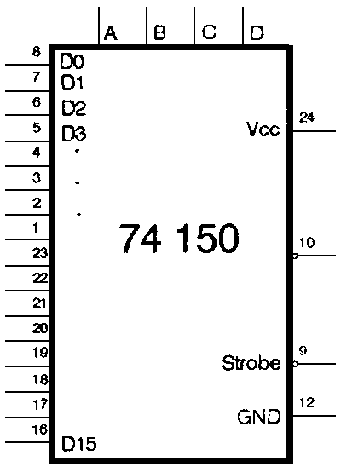
Fig. 9-1: 74 150, 16 to 1 multiplexer
No. 2 Show how to connect a 74150 (use Fig. 9-1) to implement the following Boolean equation:
No. 3 Draw a circuit with two 74150's that has the truth table like the following one:
|
A |
B |
C |
D |
Y1 |
Y2 |
|
0 |
0 |
0 |
0 |
0 |
0 |
|
0 |
0 |
0 |
1 |
1 |
0 |
|
0 |
0 |
1 |
0 |
0 |
0 |
|
0 |
0 |
1 |
1 |
0 |
1 |
|
0 |
1 |
0 |
0 |
0 |
0 |
|
0 |
1 |
0 |
1 |
1 |
1 |
|
0 |
1 |
1 |
0 |
1 |
1 |
|
0 |
1 |
1 |
1 |
1 |
1 |
|
1 |
0 |
0 |
0 |
0 |
1 |
|
1 |
0 |
0 |
1 |
1 |
0 |
|
1 |
0 |
1 |
0 |
1 |
0 |
|
1 |
0 |
1 |
1 |
1 |
0 |
|
1 |
1 |
0 |
0 |
0 |
0 |
|
1 |
1 |
0 |
1 |
1 |
0 |
|
1 |
1 |
1 |
0 |
1 |
1 |
|
1 |
1 |
1 |
1 |
0 |
0 |
|
| ||||||||||||||||||||||||||||||||||||||||||||||||||||||||||||||||||||||||||||||||||||||||||||||||||||||
Third Evaluation
No. 1 At a distribution point of a conveyer belt a flap which is controlled by a counter circuit is to divert arriving piece-goods always six to the left and four to the right.

Fig. 1
The counting pulses T are supplied by a light barrier immediately before the diverting flap. The flap opens the way to the left if the control instructions are x = 1, y = 0 and to the right when x = 0, y = 1
Develop the truth table. Use the sum of product method. For the simplification use a Karnaugh map. Design the logic circuit.
Take a decimal counter with four output lines (20, 21, 22, 23).
No. 2 Sketch an asynchronous mod 16 counter. Use JK-MS flip flops.
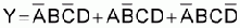
No. 3 Show how to connect a 74150 multiplexer (Fig. 2) to implement the following boolean equation:


Fig. 2
No. 4 Input signals R and T are low in Fig. 3. Which is the active output line when A B C D = 0011?
No. 5 To get the y9 output line active in Fig. 3, what are the input signals you need?

Fig.
3
|
| ||||||||||||||||||||||||||||||||||||||||||||||||||||||||||||||||||||||||||||||||||||||||||||||||||||||
Answers to Evaluation Problems
First evaluation:
No. 1
|
A |
B |
C |
X | |
|
0 |
0 |
0 |
0 | |
|
0 |
0 |
1 |
1 | |
|
0 |
1 |
0 |
0 | |
|
0 |
1 |
1 |
1 |
X = A B + C |
|
1 |
0 |
0 |
0 | |
|
1 |
0 |
1 |
1 | |
|
1 |
1 |
0 |
1 | |
|
1 |
1 |
1 |
1 | |
No. 3
|
B |
|
C (A + B) |
|
|

No. 4
|
A |
B |
C |
D |
X |
|
0 |
0 |
0 |
0 |
. |
|
. |
. |
. |
. |
. |
|
. |
. |
. |
. |
. |
|
1 |
1 |
0 |
1 |
1 |
|
1 |
1 |
1 |
0 |
1 |
|
1 |
1 |
1 |
1 |
1 |

No. 5

Second evaluation:
No. 1
|
A |
B |
C |
X | |
|
0 |
0 |
0 |
0 | |
|
0 |
0 |
1 |
0 | |
|
0 |
1 |
0 |
0 | |
|
0 |
1 |
1 |
1 |
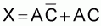
Q = AB + AC |
|
1 |
0 |
0 |
0 | |
|
1 |
0 |
1 |
1 | |
|
1 |
1 |
0 |
0 | |
|
1 |
1 |
1 |
1 | |
No. 2
| |
A |
B |
C |
T |
U |
V |
W |
X |
Y |
Z |
|
0 |
0 |
0 |
0 |
X |
X |
X |
X |
X |
X |
X |
|
1 |
0 |
0 |
1 |
0 |
0 |
0 |
1 |
0 |
0 |
0 |
|
2 |
0 |
1 |
0 |
1 |
0 |
0 |
0 |
0 |
0 |
1 |
|
3 |
0 |
1 |
1 |
1 |
0 |
0 |
1 |
0 |
0 |
1 |
|
4 |
1 |
0 |
0 |
1 |
0 |
1 |
0 |
1 |
0 |
1 |
|
5 |
1 |
0 |
1 |
1 |
0 |
1 |
1 |
1 |
0 |
1 |
|
6 |
1 |
1 |
0 |
1 |
1 |
1 |
0 |
1 |
1 |
1 |
|
7 |
1 |
1 |
1 |
x |
x |
x |
x |
x |
x |
x |
|
T = Z |
T = B + A |
V = A |
|
U = Y | | |
|
V = X |
U = AB |
W = C |
Second evaluation:

No. 3

No. 4
Third evaluation:
No. 1
|
clock |
A |
B |
C |
D |
X |
Y |
|
0 |
0 |
0 |
0 |
0 |
1 |
0 |
|
1 |
0 |
0 |
0 |
1 |
1 |
0 |
|
2 |
0 |
0 |
1 |
0 |
1 |
0 |
|
3 |
0 |
0 |
1 |
1 |
1 |
0 |
|
4 |
0 |
1 |
0 |
0 |
1 |
0 |
|
5 |
0 |
1 |
0 |
1 |
1 |
0 |
|
6 |
0 |
1 |
1 |
0 |
0 |
1 |
|
7 |
0 |
1 |
1 |
1 |
0 |
1 |
|
8 |
1 |
0 |
0 |
0 |
0 |
1 |
|
9 |
1 |
0 |
0 |
1 |
0 |
1 |
| |
Don't care conditions | | ||||


Figure

No. 2
No. 3
- Connect Vcc to 5V
- Connect GND and Strobe to ground
- Connect D5, D10, and D14 to ground
- Connect all other D inputs to 5V
No. 4
No output line is active, chip is disabled ® Strobe is high!
No. 5
-R and T ® high
-ABCD = 1001